O que você está procurando?
Pesquisas populares
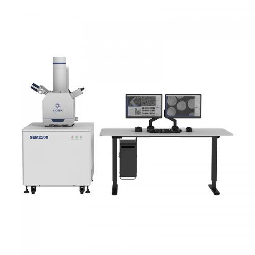
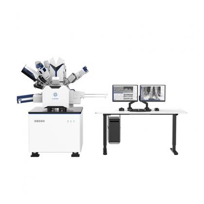
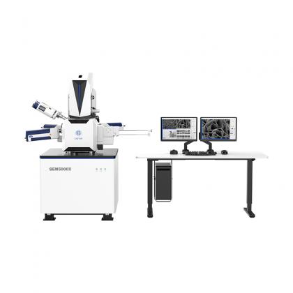
- Fabricante de microscópio eletrônico de varredura de emissão de campo, fornecedor global
- Detectores SEM EDX, EDS, EBSD, BSE, CL, STEM
- Aplicações do microscópio de força atômica do diamante do quantum do magnetômetro do nanovolt QDAFM
- fabricante de microscópio central de varredura ciqtek NV
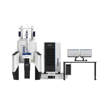
- Fornecedor global de magnetometria de varredura NV
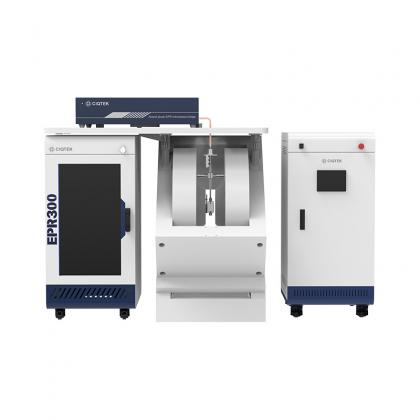
- Fornecedor global de espectroscopia de ressonância paramagnética de elétrons de pulso de banda X
- Melhor preço de espectroscopia de ressonância paramagnética eletrônica
- Espectroscopia EPR banda X com criostato
- Espectroscopia de ressonância paramagnética eletrônica de banda W melhor preço
- Espectroscopia de ressonância de rotação eletrônica de banda W, melhor preço