


Failure analysis rarely starts with a perfect sample.
At ISTFA 2026, the 52nd International Symposium for Testing and Failure Analysis, many of our conversations began with real-world challenges: buried defects, difficult cross sections, subtle material contrast, and structures that require more than surface-level imaging.
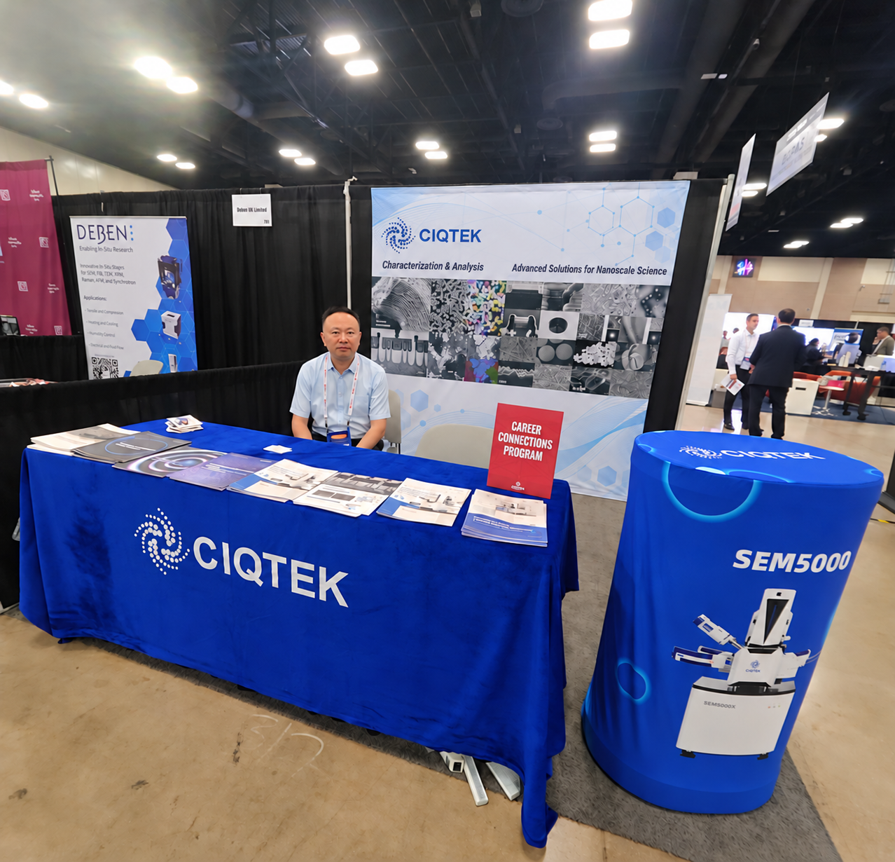
From October 4 to 8 in San Antonio, Texas, CIQTEK U.S. Electron Microscopy Team met with failure analysis engineers, semiconductor researchers, and microscopy specialists at Booth #317 to discuss practical SEM and FIB-SEM workflows.
From Surface Imaging to Buried Defect Analysis
Discussions at ISTFA covered a wide range of applications, including:
- Semiconductor device and wafer inspection
- High-resolution low-kV imaging
- Surface defect and morphology analysis
- Material contrast and contamination analysis
- Site-specific cross-sectioning
- Buried defect and interface characterization
SEM helps reveal surface morphology, interfaces, particles, and material contrast, while FIB-SEM extends the analysis beneath the surface through precise milling and targeted cross-section preparation.
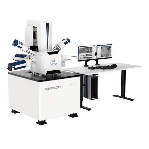
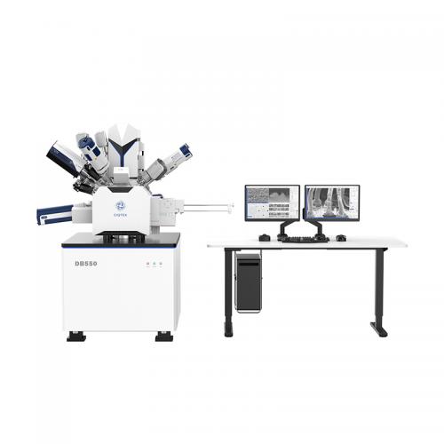
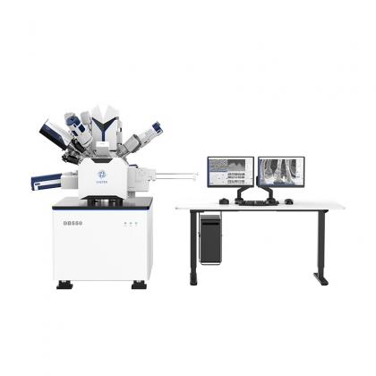
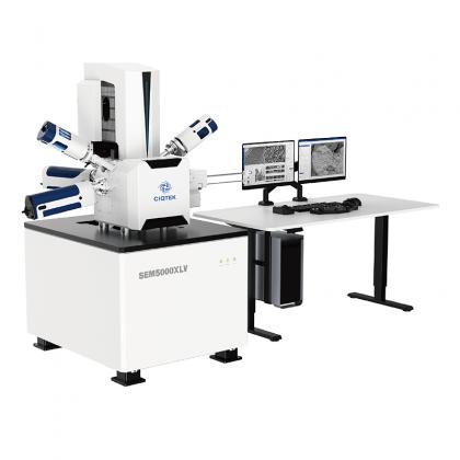
CIQTEK also introduced its electron microscopy solutions, including the SEM5000 Series and DB550 FIB-SEM, for semiconductor failure analysis and advanced materials characterization.
Valuable Conversations at Booth #317
Beyond instrument specifications, many discussions focused on real laboratory needs such as sample type, imaging conditions, detector configuration, workflow efficiency, and cross-section quality.
These conversations gave our team valuable insight into the challenges faced by semiconductor and failure analysis laboratories in the U.S.
Thank you to everyone who visited our booth and shared your applications and ideas with us.
We look forward to continuing the conversation and supporting more laboratories with practical electron microscopy solutions for failure analysis and defect characterization.